目录
What is PCB?
PCBs ( Printed Circuit Boards ) are foundational to modern times electronics, fixing and connecting electronic components precisely. The process steps of PCB manufacturing include many many many considerate steps, each strict to keep the final PCBs’ features and reliability. This blog article describes the necessary steps of the PCB fabrication process and highlights best practices and technical insights that can improve project outcomes. LHD PCB can produce PCBs from 0 layers to 32 layers, we have rich experience in producing multi-layer PCBs.
The following is an introduction to the PCB fabrication process:
Step 1: Design planning and projected production planning
The PCB fabrication process starts with a clear design and planning. PCB design engineers use sophisticated design software to make printed circuit board blueprints that include circuit pattern layout, component placement, and electrical connections between them. Careful consideration of PCB board size, layer counts, and functionality is critical to avoid complications during fabrication. Prototype is also part of this phase, allowing potential problems to be identified and corrected early in the design phase. LHD PCB can provide a one-stop service for PCBA, if you need any kind of design service, please feel free to contact us.
Step 2: PCB Fr4 Sheet Material selection
Finding the right and good Fr4 materials is necessary for PCB work performance and durability. Normal PCB Fr4 sheet materials include fiberglass, composite epoxies, and different types of copper. PCB material selection affects the heat dissipation, electrical insulation properties, and structural integrity of the PCB boards, so it is necessary to find based on the specific requirements of your device. LHD PCB have kinds Fr4 , such as S1141, S1000, It-180, KB6160, KB6165, etc..
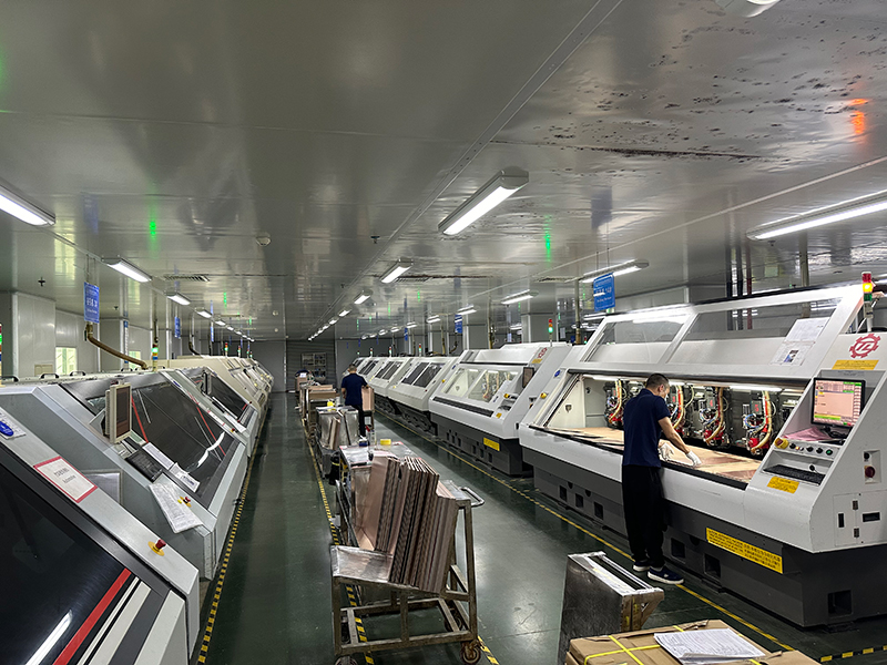
Step 3: Drilling and Photolithography
All Fr4 sheet material needs drilling at first, then plating copper in the holes. After plating copper in the holes, we need to print a copper pattern in the copper layer, this step is photolithography. Photolithography is a necessary step in PCB fabrication where the PCB board’s design is transferred onto a photosensitive material applied to the substrate. This process includes covering the substrate with a light-sensitive chemical layer, placing a photomask over the substrate, and exposing it to ultraviolet light. The exposed areas harden, while the unexposed parts are washed away, creating a precise stencil of the PCB design.
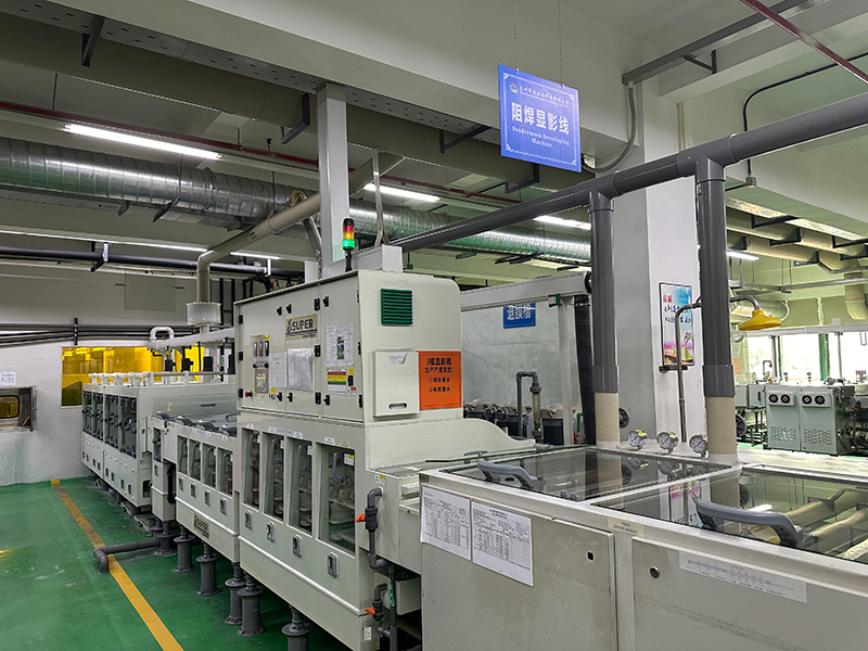
Step 4: Etching Copper Pattern
All the photolithography is produced in the yellow room which can prevent the sunlight get into the room. These films in the copper can get wrong if they are covered by sunlight. After the photolithography process, the etching copper process removes the unwanted metal from the board, leaving only the desired traces of copper or other conductive materials. This step must be carefully controlled to ensure accuracy and prevent damage to the remaining circuitry. Various etching chemicals can be used, each requiring specific handling and disposal methods to minimize environmental impact. LHD PCB factory has a VCP plating line which can ensure all PCB plating is good and the etching process will be easy and better.
Step 5: Lamination process-the necessary step for multi-layer PCB
LHD PCB can produce PCBs from 0 layers to 32 layers, we have rich experience in producing multi-layer PCBs. For multi-layer PCBs, individual layers containing the circuitry are stacked and bonded. Each layer is aligned precisely by rivet before lamination, using heat and pressure to fuse them together into a single structure. This step is necessary for multi-layer boards as it ensures that the layers are perfectly aligned and securely bonded, enhancing the board’s overall durability and functionality.
Step 6: Drilling and Plating
For the multi-lay PCBs, once the layers finish the lamination, drilling is performed to create vias, which are holes that allow electrical connection between different copper layers of the PCB. Post-drilling, the board undergoes plating, where a thin copper layer of about 2um is deposited into the walls of the drilled vias, strengthening the connections and ensuring conductivity throughout the board. LHD PCB factory has a VCP plating line which can ensure all PCB plating is good and the etching process will be easy and better.
Step 7: Print the Solder Mask on the PCBs
Almost all the PCBS have the solder mask, usually green in color, which is applied to the PCB’s surface, covering the entire board except for the pads and holes where soldering components are necessary. But LHD PCB can support many color solder masks, such as red, blue, black, matte green, matte red, matte black, matte blue, and gray, we can also make pink and transparent colors. This mask prevents accidental solder bridges between closely spaced solder pads, which can lead to short circuits.
Step 8: Surface Finish Treatment and Silkscreening
The surface finish is applied to enhance the solderability and protect the exposed copper circuitry from oxidation and corrosion. Common finishes include HASL (Hot Air Solder Leveling) and ENIG (Electroless Nickel Immersion Gold). LHD PCB can produce more than this, such as LFHASL, ENEPIG, OSP, Immersion Tin, Immersion Ag, gold fingers, etc.
Finally, silkscreening adds labels and markings on the PCB for identifying components and test points, facilitating easier assembly and maintenance. Also, the silkscreen can have many colors, such as white, black, yellow, red, etc.
Conclusion:
The PCB fabrication process is intricate and requires precision at every step. Understanding these stages is crucial for electronics manufacturers and engineers aiming to produce high-quality, reliable PCBs. By carefully considering each phase, from design to finishing, you can ensure your PCBs meet the stringent standards required for today’s electronic devices.
0